

In this paper we report the simulation-based design of experiment (DoE) study for three different types of III-V based pin photodetectors operating at various wavelengths. Our DoE work shows that the optimal configuration for each device is strongly determined by the wavelength at which we are aiming to operate the photodetector and that a trade-off […]
D04–Ge-on-Si waveguide photodetectors: multiphysics modeling and experimental validation
This work compares a multiphysics modeling approach with experimental measurements of two Ge-on-Si butt-coupled waveguide photodetectors. The coupled three dimensional electromagnetic and electrical simulation of the frequency response shows promising agreement with the measurements at 1310 nm, and provides detailed information about significant microscopic quantities, such as the spatial distribution of the optical generation rate.
D03–Plasmonic nanorods for enhanced absorption in mid-wavelength infrared detectors
The absorption properties of HgCdTe based infrared detectors can be greatly increased in the mid-infrared band, by incorporating nanostructured plasmonic arrays on the illuminated detector face. The array periodicity, combined with the excitation of surface plasmon-polariton stationary modes, enhances the absorption efficiency by a substantial amount, allowing to reduce in turn the HgCdTe absorption thickness.
D01–Probability Theory of Single-Carrier Avalanche in HgCdTe APDs as a Stochastic Process
Recent researches have proven that HgCdTe is a good material to acquire both high multiplication and low excess noise factor at the same time in avalanche photodiodes (APDs). As a pseudo-binary narrow bandgap semiconductor material, HgCdTe exhibits high conduction band nonparabolicity as well as strong alloy scattering, especially for hot electrons, which changes the dynamics […]
D02–Performance of Plasmonic Side-Coupled Waveguide Photodetector with Varying Schottky Barrier Height
The impact of Schottky barrier height (SBH) on the performance of a side-coupled plasmonic waveguide photodetector (WGPD) is theoretically investigated by 3D optoelectrical simulations. A general decrease of the cut-off frequency is observed for all studied barrier heights (0.1 eV to 0.6 eV), most pronounced in the range (0.3 – 0.4) eV. The degradation is […]
N09–Luminescence Decay Kinetics of Electron-Hole Plasma in II-VI Epitaxial Layers and Micropowders
The luminescence decay kinetics of epitaxial layers of ZnSe and micropowders of ZnSe and CdS were measured at room temperature and at high levels of optical excitation. Comparison of the experimental results with the theoretically calculated decay kinetics showed good agreement for the initial moment of time at high concentrations of nonequilibrium charge carriers.
N08–Dependence of conduction mechanism on bias and temperature in quantum-dot based electroluminescent devices
Quantum dots (QDs) provide some unique properties which make them preferable over other luminescent materials, one such property being adjustable and sharp emission which makes it an interesting candidate for electroluminescent devices. A QD based electroluminescent device has been taken into consideration in this theoretical study. The effect of the bias, temperature, the presence of […]
N07–Short Pulses from QD Laser Excited State
For the first time gain-switched short pulse generation with a width of 25-40 ps from excited state is demonstrated applying an external optical Gaussian beam to the excited state of InAs-InP-(113)B quantum dot laser.
N06–Optical properties of a waveguide-fed plasmonic nano-array through approximated scattering theory
We analyze the optical scattering properties of an array of Au nano-cylinders fabricated upon an ion-exchanged waveguide. The integrated systems is considered for fluoroscopy and Raman spectroscopy. Absorption, scattering and extinction have been calculated through a combination of Finite Difference Time Domain (FDTD) method and scattering theory. While a portion of the excitation signal interacts […]
N05–Modeling the effects of p-modulation doping in InAs quantum dot devices
A modeling routine has been developed to quantify the effects of p-modulation doping in the waveguide core region of InAs quantum dot (QD) devices. Utilizing one dimensional approximations, simulated outputs of reverse and forward devices are simulated providing insight into absorption and gain properties.
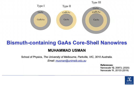
N04–Bismuth-containing GaAs core-shell nanowires
This work theoretically investigates the electronic and optical properties of GaBixAs1–x/GaAs core–shell and GaAs/GaBixAs1–x/GaAs multi-core–shell nanowires. Our results show a large tuning of absorption wavelength (0.9 µ to 1.6 µ) by varying Bi composition and/or nanowire diameters. The computed polarisation dependent optical spectra indicate the possibility to incorporate such nanowires in photonic devices desiring isotropic […]
N03–Numerical and Experimental Characterization of Chirped Quantum Dot-based Semiconductor Optical Amplifiers
We present a model for the description of the dynamical behavior of Quantum Dot (QD) based Semiconductor Optical Amplifiers (SOAs) under injection of optical pulses. The model uses a Time Domain Traveling Wave (TDTW) approach to describe the optical field in the amplifier, and allows us to consider chirped QD materials by the inclusion of […]
N02–Wave-function engineering in (In,Ga)As/(In,Al)As core/shell nanowires
We study the electronic properties of In0.53Ga0.47As/InxAl1–xAs core/shell nanowires for light emission in the telecommunication range. In particular, we systematically investigate the influence of the In content x of the InxAl1–xAs shell and the diameter d of the In0.53Ga0.47As core on strain distribution, transition energies, and the character of the hole wave function. We show […]
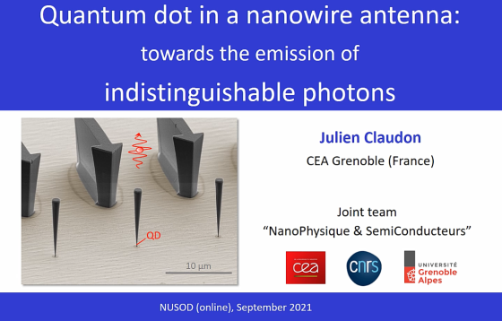
N01–Nanowire antennas embedding single quantum dots: towards the emission of indistinguishable photons
Nanowire antennas embedding a single semiconductor quantum dot (QD) represent an appealing solid-state platform for photonic quantum technologies. We present recent work aiming at generating indistinguishable photons with this system. We first investigate decoherence channels that spectrally broaden the QD emission, and discuss in particular the impact of nanowire thermal vibrations. We also develop nanowire […]
NM07–Design and Analysis of Slow Light Device based on Double Quantum Dots Tunneling Induced Transparency
Slow light Transparency window can be achieved with the help of Electromagnetically Induced Transparency (EIT) method and Tunneling Induced Transparency (TIT) method accompanied by observing tunneling effect between InAs quantum dot structure with energy gap of 0.35 eV and a thin layer of GaAs potential barrier with energy gap of 1.42 eV. By investigating different […]
NM06–Simulation aided design of a human wrist rotation recognition system combining IMU sensor data with Visible Light Communication
Wrist worn mobile sensors have proven to be applicable for various applications, including fitness tracking or gesture recognition. In time- and security-critical application scenarios, the commonly used Radio frequency based communication technologies may pose a bottleneck for further advancements. In this work, we present a simulation environment implemented in Matlab/Simulink that enables the precise simulation […]
NM05–Modelling of mixed-phase MAPbI3
Both x-ray diffraction (XRD) and photoluminescence (PL) characterizations of methylammonium lead iodide perovskite (MAPbI3) reveal signatures of a coexistence of the tetragonal and orthorhombic phases over a wide range of temperatures, suggesting that the phase transition does not happen sharply at a temperature of 164 K as reported in literature. To understand the causes of […]
NM04–Strain-balanced GaAs(1-x)Bi(x)/GaN(y)As(1-y) W-type quantum wells for GaAs-based 1.3-1.6µm lasers
Highly-mismatched alloys constitute a promising approach to extend the operational range of GaAs-based quantum well (QW) lasers to telecom wavelengths. This is challenging using type-I QWs due to the difficulty to incorporate sufficient N or Bi via epitaxial growth. To overcome this, we investigate a novel class of strain-compensated type-II QWs combining electron-confining, tensile strained […]
NM03–Tight binding simulations of tetragonal MAPbI3 domains within orthorhombic phase
Very recent photoluminescence studies, investigating the tetragonal-to-orthorhombic phase transition of MAPbI3, demonstrated the presence of residual tetragonal phase far below the transition temperature, yielding spectral signatures from quantum confined tetragonal domains. We present a theoretical model of the coexistence of tetragonal and orthorhombic MAPbI3, based on tight binding simulations. The tight binding parameters are derived […]
NM01–Machine Learning & multiscale simulations: toward fast screening of organic semiconductor materials
Organic semiconductor devices promise cost-efficient processability at low temperatures, but the usually amorphous materials suffer from low charge carrier mobility. The search for high mobility organic semiconductor materials has thrived data science and Machine Learning approaches to screen the vast amount of possible organic materials. We present a multiscale simulation model based on machine learned […]
P01–Design of a computer-generated waveguide hologram for integrated free space sensing
In this work we present a design of a computer generated waveguide hologram coupler with an ultra-long working distance and wavelength multiplexing in the near infrared. An approximation method to compute the scalar field from a detour phase hologram is presented. The accuracy is comparable to FDTD but it is achieved much faster. Coupling efficiency […]
IS01–Improved Phase Detection in On-Chip Refractometers
An improved phase detection scheme for Mach-Zehnder and bimodal interferometers is presented. By using a 90° hybrid, always two outputs operate at a highly sensitive point and the phase-shift-unambiguousness is extended to a range of 2π. The phase detection is independent of mode attenuations and input power fluctuations.
MM01–Connecting atomistic and continuum models for (In,Ga)N quantum wells: From tight-binding energy landscapes to electronic structure and carrier transport
We present a multi-scale framework for calculating electronic and transport properties of nitride-based devices. Here, an atomistic tight-binding model is connected with continuum based electronic structure and transport models. In a first step, the electronic structure of (In,Ga)N quantum wells is analyzed and compared between atomistic and continuum-based approaches, showing that even though the two […]
LED01–Effect of Inhomogeneous Broadening in Deep Ultraviolet Light Emitting Diodes
Due to their small dimensions deep ultraviolet (DUV) light emitting diodes (LED) are highly attractive light sources for environmental and medical applications. DUV LEDs generate light in active quantum wells (QW) made of Aluminium Gallium Nitride. The QWs are not lattice matched to the substrate and only few monolayers thick making them susceptible to compound […]
LD01–Multimode Dynamics and Frequency Comb Generation in Quantum Cascade Lasers
In this talk I will discuss how resonant light-matter interaction in the gain medium of quantum cascade lasers gives rise to a rich nonlinear multimode dynamics and a variety of phase-locked multimode regimes, most notably optical frequency combs with separation between the comb lines changing from one to many dozen round-trip frequencies. I will review […]

